MCS6500
Microcomputer Family
Programming Manual
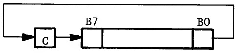
CHAPTER 10 SHIFT AND MEMORY MODIFY INSTRUCTIONS 10.0 DEFINITION OF SHIFT AND ROTATE In many cases operations of the control systems must operate a bit at a time. Data is often available only bit-serial and sometimes sequential bit operations are the only way to solve a particular problem. In addition to that, in order to combine bits into a field, shift and rotate instructions are necessary. Multiply and divide routines all require the ability to move bits relative to one another in a full multiple byte field. The shift instruction is one that takes a register such as the accumulator and moves all of the bits in the accumulator 1 bit to the right or 1 bit to the left. Examples of the shift and rotate instructions in the MCS650X are shown below:
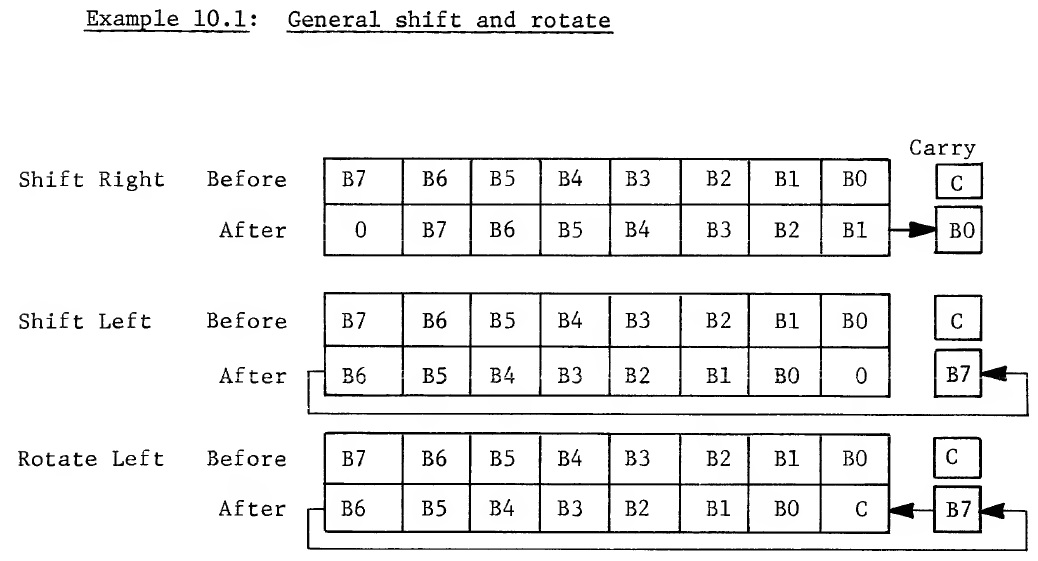
As you can see from our example, moving data 1 bit to the right is called shift right. The natural consequence of the shift right is that the input bit or high order bit in this case is set to 0. Moving the data in the register 1 bit to the left is called shift left. In this case, the is inserted in the low order position. These are the 2 shift capabilities that exist in the MCS650X microprocessor. It should be noted that in both cases, the bit that is shifted from the register, the low order bit in shift right, and the high order bit in shift left, is stored in the carry flag. This is to allow the programmer to test the bit by means of the carry branches that are available and also to allow the rotate capability to transfer bits in multiple precision shifts. The second part of the multiple precision shift instruction is the rotate which is shown in Example 10.1, in which the value of the carry bit becomes the low order bit of the register, and the output bit from the shift is stored in carry. 10.1 LSR - LOGICAL SHIFT RIGHT This instruction shifts either the accumulator or a specified memory location 1 bit to the right, with the higher bit of the result always being set to 0, and the low bit which is shifted out of the field being stored in the carry flag. The symbolic notation for LSR is
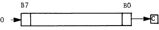
The shift right instruction either affects the accumulator by shifting it right 1 or is a read/modify/write instruction which changes a specified memory location but does not affect any internal registers. The shift right does not affect the overflow flag. The N flag is always reset. The Z flag is set if the result of the shift is and reset otherwise. The carry is set equal to bit of the input. LSR is a read/write/modify instruction and has the following addressing modes: Accumulator; Zero Page; Zero Page, X; Absolute; Absolute, X. 10.2 ASL - ARITHMETIC SHIFT LEFT The shift left instruction shifts either the accumulator or the address memory location 1 bit to the left, with the bit always being set to and the bit 7 output always being contained in the carry flag. ASL either shifts the accumulator left 1 bit or is a read/modify/write instruction that affects only memory. The symbolic notation for ASL is
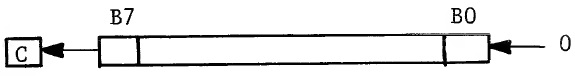
The instruction does not affect the overflow bit, sets N equal to the result bit 7 (bit 6 in the input) , sets Z flag if the result is equal to 0, otherwise resets Z and stores the input bit 7 in the carry flag. ASL is a read/modify/write instruction and has the following addressing modes: Accumulator; Zero Page; Zero Page,X; Absolute; Absolute,X 10.3 ROL - ROTATE LEFT The rotate left instruction shifts either the accumulator or addressed memory left 1 bit, with the input carry being stored in bit and with the input bit 7 being stored in the carry flags. The symbolic notation for ROL is
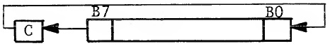
The ROL instruction either shifts the accumulator left 1 bit and stores the carry in accumulator bit or does not affect the internal registers at all. The ROL instruction sets carry equal to the input bit 7, sets N equal to the input bit 6, sets the Z flag if the result of the rotate is , otherwise it resets Z and does not affect the overflow flag at all. ROL is a read/modify/write instruction and it has the following addressing modes: Accumulator; Zero Page; Zero Page,X; Absolute; Absolute, X. 10.4 ROR - ROTATE RIGHT (Available on Microprocessors after June, 1976) The rotate right instruction shifts either the accumulator or addressed memory right 1 bit with bit shifted into the carry and carry shifted into bit 7. The symbolic notation for ROR is
The ROR instruction either shifts the accumulator right 1 bit and stores the carry in accumulator bit 7 or does not affect the internal registers at all. The ROR instruction sets carry equal to input bit 0, sets N equal to the input carry and sets the Z flag if the result of the rotate is 0; otherwise it resets Z and does not affect the overflow flag at all. ROR is a read/modify/write instruction and it has the following addressing modes: Accumulator; Zero Page; Absolute; Zero Page,X; Absolute, X. 10.5 ACCUMULATOR MODE ADDRESSING As indicated, all of the shift instructions can operate on the accumulator. This is a special addressing mode that is unique to the shift instructions and operates with the following set of operations: Example 10.2: Rotate accumulator left External Internal Cycle Address Bus Data Bus Operation Operation 1 100 OP CODE Fetch Next Finish Previous OP CODE Operation; Increment PC to 101 2 101 Next Fetch Discarded Decode current Instruction; OP CODE OP CODE Hold P-Counter 3 101 Next Fetch Next Shift Through the OP CODE OP CODE Adder 4 102 ? Fetch Second Store results into A; Byte Interpret Next OP CODE As we can see, the accumulator instructions have the same effect as the single-byte non-stack instructions in the sense that the instruction contains both the OP CODE and the register in which the operations are going to be performed; therefore, in cycle 2, the microprocessor holds the program counter and in cycle 3, fetches the same program counter location and starts the next instruction operation. At the same time, it is transferring the results from the adder into the accumulator; this is because of the lookahead and pipelining characteristics of the MCS650X. The accumulator shift and rotate operations take only 2 cycles and 1 byte of memory. 10.6 READ/MODIFY/WRITE INSTRUCTIONS The MCS650X has a series of instructions which allow the user to change the contents of memory directly with a single instruction. These instructions include all of the shift, rotate, increment and decrement memory instructions. The operation of each of these instructions is the same in that the addressing mode that is defined for the instruction is implemented the same way as if for normal instructions. After the address has been calculated, the effective address is used to read the memory location into the microprocessor arithmetic unit (ALU) . The ALU performs the operation and then the same effective address is used to write the results back into memory. The most difficult operation is the addressing mode Absolute Indexed which is illustrated in Example 10.3 for the rotate left instruction, ROL: Example 10.3: Rotate memory left Absolute,X External Internal Cycle Address Bus Data Bus Operation Operation 1 100 OP CODE Fetch Finish Previous OP CODE Operation; Increment PC to 101 2 101 ADL Fetch ADL Decode current Instruction, Increment PC to 102 3 102 ADH Fetch ADH Add ADL+X, Increment PC to 103 4 ADH, ADL + X ? False Read Add Carry from Previous Add to ADH 5 ADH + C Data Fetch Value ADL + X 6 ADH + C ? Destroy Perform Rotate, ADL + X Memory Turn on Write 7 ADH + C Shifted Store Set Flags ADL + X Data Results 8 103 OP CODE Fetch Next Increment PC to 104 OP CODE Cycle 4 is a wasted cycle because read/modify/write instruction should wait until the carry had been added to the address high in order to avoid writing a false memory location. This is the same logic that is used in the store instruction in which the look-ahead or the short cut addressing mode is not taken advantage of. Cycle 4 is an intermediate read, and cycle 5 is when the actual data that is going to be operated on is read. The address lines now hold at that address for cycles 5, 6 and 7. The microprocessor signals both itself and the outside world those operations during which it will not recognize the ready line. It does this by pulling the Write line. The Write line is pulled in cycle 6 because data is written into the memory location that is going to be written into again in cycle 7 with correct data. Because data bits read from memory have to be modified and returned, there is no pipelining effect other than the overlap of the adding in the address low and index register. The 7 cycles it takes to perform read/ modify/write Absolute Indexed, X instruction is the worst case in timing for any section of the machine except for interrupt. This unique ability to modify memory directly is perhaps best illustrated by the coding in Example 10.4 which is used to shift a 4-bit BCD number, which has been accumulated in the high 4 bits of the accumulator as part of the decoding operation, from the accumulator- into a memory field. Figure 10.1 is a flow chart of this example. Examples such as this often occur in point-of-sale terminals and other machines in which BCD data is entered sequentially. This example assumes that the value is keyboard entered, through which data is entered into the accumulator from left to right but has to be shifted into memory from right to left. The value in the field before the shift is a 1729 which after the shift will be a 17,295.
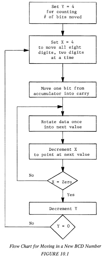
Example 10.4: Move a new BCD number into field Before After Field 00 00 00 01 17 72 29 95 Accumulator 50 00 Coding Bytes Instruction 2 LDY 4 2 LOOP-2 LDX 4 set up for 4 moves 1 ASLA 3 LOOP-1 ROL Price-1, X 1 DEX shift the field 1 bit 2 BNE LOOP-1 1 DEY shifts four times. 2 BNE LOOP-2 14 bytes There are several new concepts introduced in this example; the first is the use of index register Y as just a counter to count the number of times the character has been bit-shifted. It is a common approach to use bit shifts, as is implemented in the MCS650X family, to shift data into memory. The power of being able to communicate directly in memory is shown by shifting bits from one byte to the next byte using a single ROL indexed instruction. This example uses a loop within a loop and it should be noted that LOOP 1 occurs 4 times for every time LOOP 2 occurs. The internal loop is very important in the sense that this loop executes 16 times for the problem; therefore, its execution time should be optimized. In addition to having the ability to shift and rotate memory, the MCS650X has the ability to increment and decrement memory locations. 10.7 INC - INCREMENT MEMORY BY ONE This instruction adds 1 to the contents of the addressed memory location. The symbolic notation is M + 1 → M. The increment memory instruction does not affect any internal registers and does not affect the carry or overflow flags. If bit 7 is on as the result of the increment, N is set, otherwise it is reset; if the increment causes the result to become 0, the Z flag is set on, otherwise it is reset. The addressing modes for increment are; Zero Page; Zero Page,X; Absolute; Absolute, X. 10.8 DEC - DECREMENT MEMORY BY ONE This instruction subtracts 1, in two's complement, from the contents of the addressed memory location. Symbolic notation for this instruction is M - 1 → M. The decrement instruction does not affect any internal register in the microprocessor. It does not affect the carry or overflow flags. If bit 7 is on as a result of the decrement, then the N flag is set, otherwise it is reset. If the result of the decrement is 0, the Z flag is set, otherwise it is reset. The addressing modes for decrement are: Zero Page; Zero Page,X; Absolute; Absolute, X. In many examples through the report, we have used the ability to increment and decrement registers in the microprocessors. The advantages of incrementing and decrementing in memory are that it is possible to keep external counters or to directly influence a bit value by means of these instructions. It is sometimes useful during I/O instructions. 10.9 GENERAL NOTE ON READ/MODIFY/WRITE INSTRUCTIONS The ability to read, modify and write memory is unique to MCS6500 class microprocessors. The usefulness of the instructions is limited only by the user's approach to organizing memory. Even though the instructions are fairly long in execution, they are significantly shorter than having to load and save other registers to perform the same function. Experience in organizing programs to take advantage of this manipulation of memory will allow the user to fully appreciate the power of these instructions.