MCS6500
Microcomputer Family
Programming Manual
CHAPTER 11 PERIPHERAL PROGRAMMING 11.0 REVIEW OF MCS6520 FOR I/O OPERATIONS It should be noted that in the following discussions, the major difference between the MCS6530 I/O and the main register of the MCS6520 is that the extra bit in the control register need not be used in the MCS6530. All registers in the MCS6530 are directly addressable.
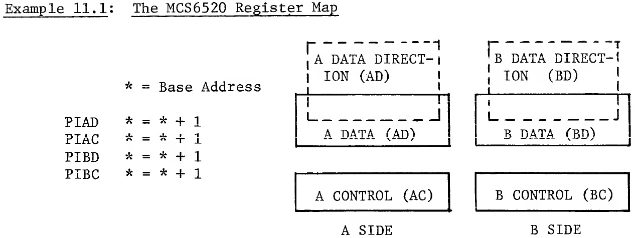
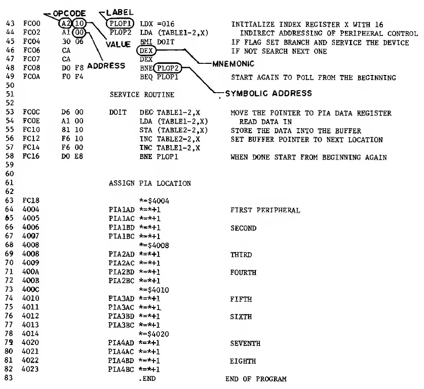
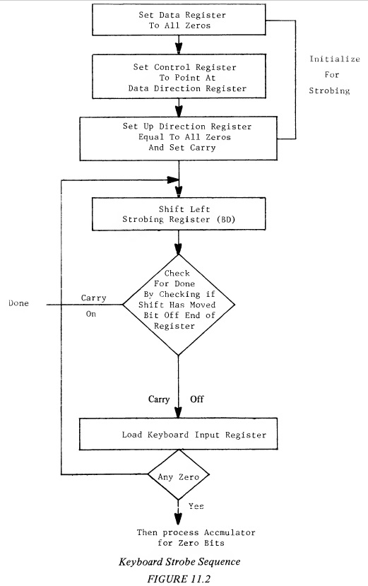
In Example 11.1 a programming form to describe the PIA is shown. The programming form is used in the Cross-Assembler and Resident Assembler with the MCS650X product family. The notation * = is used to define any location. The notation means that the assembler instruction counter is set equal to the value following the equal sign. The expression * = * + 1 causes the assembler to recognize that there is one byte of memory associated with the term; therefore, we can see that the definition of the four registers PIAD, PIAC, PIBD and PIBC are consecutive memory locations starting at some base address, with the first byte addressed as PIAD, the second byte addressed as PIAC, the third byte addressed as PIBD, and the fourth byte as PIBC. This is a normal way a MCS6520 would be organized and this is the way the programming form should be set up. The base address is picked up by an algorithm described in the hardware manual but normally it is a value between 4004 and 4080 Hex. Each MCS6520 is given a base address which works progressively up from 4004 Hex. In Example 11.1 two registers are shown in dotted lines. This is because each of the A DATA (AD) and B DATA (BD) parts of the MCS6520 are actually two registers having the same address, one which specifies the direction of each of the input/output paths (the Data Direction Register) , the second one which is actually the connection to the input/ output paths (the Data Register). Because of pin limitations on the MCS6520, the microprocessor can only directly address one of the registers at a time. Differentiation as to which register is being connected to the microprocessor is a function of bit 2 in the respective control register (AC and BC) . If bit 2 is off, the Data Direction Register is being addressed; if it is on, the Data Register is being addressed. During the initialization sequence, therefore, the MCS6520 starts out with all registers at zero. This means that the microprocessor is addressing the Data Direction Register. The PIA initialization is done by writing the direction of the pins into the Data Direction Register CAD, BD) and then setting on the control flag as described below. After that, the program will normally be dealing with the data registers. Example 11.2: General PIA Initialization LDA # DIRECT Initialize Direction STA PIAD LDA # CONTR Initialize Control STA PIAC Example 11.2 illustrates a general form of initialization and can be completed for as many PIA's as there are in the system. 11.1 MCS6520 INTERRUPT CONTROL The MCS6520 has a basic interrupt capability which is under control of the programmer. Almost all MCS6500 I/O devices that allow interrupts have an interrupt control register that allows the user to disable the interrupt. This will keep inputs which are not necessarily active from causing spurious interrupts which must be handled by the microprocessor. Examples of this are open tape loops or other signals which have high impedance noise sensitive inputs except when connected to some kind of media. In this type of application, normally the interrupt is enabled by some physical action from the person using the device such as loading of the cassette, pushing the power-on switch, etc. In the case of the MCS6520, there are two interrupt causing conditions for each control register. Each of these interrupts concern themselves with one input pin. The Control Register allows the programmer to decide whether or not the pin is sensitive to positive edge signals or negative edge signals and whether or not an interrupt shall occur when the selected transition has occurred. It should be noted that, therefore, it is possible for a line to cause a status bit to be set without causing an interrupt. The comprehensive I/O Program in Section 11.5 uses this combination. Example 11.3: Interrupt Mode Setup Bit 7 Status Bit: Bits 1 0 Interrupt Set on Negative Edge 0 0 No Set on Negative Edge 0 1 Yes Set on Positive Edge 1 0 No Set on Positive Edge 1 1 Yes Bit 6 Status Bit: Bits 4 3* Interrupt Set on Negative Edge 0 0 No Set on Negative Edge 0 1 Yes Set on Positive Edge 1 0 No Set on Positive Edge 1 1 Yes *if bit 5 equals zero The proper combination of bits are usually determined during the design of the MCS6520 interconnection and form the constant which is loaded in the control register. The constant that is loaded in the control register should contain bit 2 on. For example, to allow bit 7 to be set on negative going signals with interrupt enable and bit 6 to be set on positive signals with interrupt disable, the control value would be Hex 15. With bit 5 on, the pin that controls bit 6 can be set as an output pin. The output pin is either controllable by the microprocessor directly or acts as a handshake to reflect the status of reads and writes of the data register. The operation of the output pins CA2, CB2 depends on how bits 5, 4, and 3 are programmed, as shown in Example 11.4. Example 11.4: CA2, CB2 Output Control CA2 Output With: Bit 5 on Bit 4 Bit 3 Low on read or write for one cycle 0 0 Low on read or write until 0 1 bit 7 on Always 0 1 0 Always 1 1 1 The decision as to whether or not to use the one cycle low until bit 7 comes on is a hardware decisions depending on the device which is hooked to the pin. It should be of interest to the programmer to note that bit 6 controls pins known as CA2 or CB2 which can be considered to be auxiliary outputs which are controlled by bit 3 assuming the processor is Example 11.5 shows the use of controlling bit 3 using AND and OR instructions; however, it should be noted that this technique applies for any individual bit in the PIA data direction register also: Example 11.5: Routine to Change CA2 or CB2 Using Bit 3 Control Set CA2 LDA PIAC ORA #$08 STA PIAC Clear CA2 LDA PIAC AND #$F7 STA PIAC Note: $ - Direction to Assembler for Hex Notation # - Direction to Assembler for Production Operator By similar techniques, every pin in the microprocessors of the MCS6520 can be controlled. There are two particular notes to remember: 1. In the MCS6520, both bit 6 and bit 7 are cleared on either side by reading of the corresponding data register if bit 6 has been set up as an input. This means that polling sequences for I/O instructions should only read the status registers and then read the data registers after the status has been determined, otherwise false clearing of the status data may occur. 2. Even though the handshake for the CB2 pin is on write of B data, a read of B data must be done to clear bit 7. 11.2 IMPLEMENTATION TRICKS FOR USE OF THEMCS6520 PERIPHERAL INTERFACE DEVICES 11.2.1 Shortcut Polling Sequences In section 9.7, the techniques for using a LOAD A to poll for interrupts was covered; however, the I/O devices on the MCS6520 can either set bit 6 or bit 7 on to cause an interrupt; therefore, a different technique needs to be used to analyze the MCS6520 to poll a series of 6520 's each one of which could have caused the interrupt. It is for this purpose that the BIT instruction senses both bit 6 and bit 7. Coding for a full poll of a PIA is as shown: Example 11.6: Polling the MCS6520 Interrupt Vector JMP STORE LDA #C0 BIT PIAAC Check for neither 6 or 7 BEQ NXT1 BMI SEVEN If 7 , go to save -- otherwise clear Process BIT 6 INTERRUPT NXTI BIT PIABC BEQ NXTZ etc. This program takes full advantage of the BIT instruction by checking for both bit 7 and 6 clear. BMI to SEVEN just checks N is on and that N is a higher priority. If bit 6 is one, the overflow bit will also be set, allowing the finish of the process seven routine to test the overflow and jump back to the process bit 6 coding. Bit 6 and bit 7 were sampled by the single BIT instruction. Speed was accomplished by loading the mask for just bit 6 and 7 into the register which allows the BEQ instruction to determine that neither of the two flags is on. This routine depends on the fact that in the MCS6520, if CA2 or CB2 is an output, bit 6 is always zero. 11.2.2 Bit Organization on MCS6520's In the microprocessor, there is a definite positional preference for the testing of single bits. In the MCS6520 Data Direction Register, it is possible to select any combinations of input/ output pins by the pattern that is loaded in the Data Direction Register. A one bit corresponds to an output and a zero bit corresponds to an input. The natural tendency would be to use MCS6520S with all eight bits organized into a byte. There is relatively little advantage to organizing this way unless the eight bits are to be treated as a single byte by the program. This is often not the case, more often the bits are a collection of switches, coils, lights, etc. On such combinations, advantage should be taken of the fact that bit 7 is directly testable so that a more useful combination of eight pins on one MCS6520 register would be seven outputs and a single input with the single input on bit 7. This organization allows the programmer to load and branch on that location without ever having to perform a bit or shift instruction to isolate a particular bit. A similar capability for setting a single bit involves the organization of data with seven inputs and a single output with a single output located in bit 0. This bit may be set or cleared by an INC or DEC instruction without affecting the rest of the bits in the register because the input pins ignore signals written from the microprocessor. Therefore, the more skilled MCS6500 programmer will often mix single outputs on bit and a single input on bit 7 with bits of the corresponding opposite type. 11.2.3 Use of READ/MODIFY/WRITE Instruction For Keyboard Encoding A rather unique use of the memory with a READ /MODIFY /WRITE operation involves setting the data register at all zeros, then using the three state output of the B side to sample a keyboard. The following Figure 11.1 shows the connection for a 64 key keyboard organized 8x8:
The B side is set up to act as a strobe so that each of the output lines will have a ground on it during one scan cycle. The eight A side data inputs are then sampled and decoded by the microprocessor giving a 64 key keyboard which is directly translatable into code. Figure 11.1 and Example 11.7 make use of the capability of the microprocessor to move a bit through the MCS6520 register location. This program also uses the compare instruction and the ability to detect a carry during a shift. Example 11.7: Coding for Strobing an 8 x 8 Keyboard Output Strobe is indicated by a one in Data Director Register. Any connection is indicated by a zero in register bit. LDA #0 STX PIABD Initialize B Data Register LDA PIABC AND #FB Initialize Control Register to STA PIABC Address Data Direction Register STX PIABC SEC Set low end bit on LOOP ROL PIABD Shift for Strobe BCS DONE LDA PIAAD if all sampled, exit CMP #FF Check for no zeros BEQ LOOP DONE ------- If any zeros, then process them. A and PIABD can now be used to find out just what key is depressed.
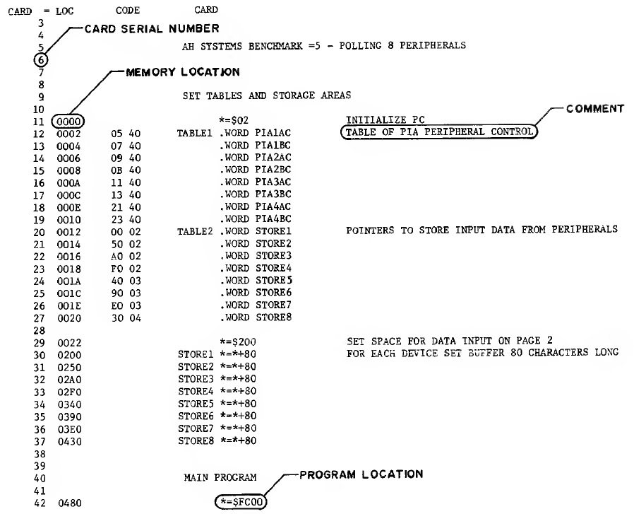
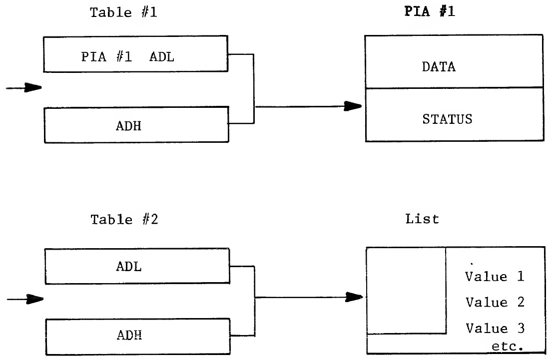
11.3 MCS6530 PROGRAMMING Although they have separate addressing, the Data Direction and Input/Output Registers operate the same as on the MCS6520, Programming of the Interval Timer has some special problems. First of all, the time is effectively located in all addresses from XXX4-XXXF. By picking the proper address, the programmer is able to control the P scale for the timeout. Initialization of the Interval Timer is done by a LOAD A followed by STORE A into the timing count. The value stored in the timing counter represents the number of states which the counter will count through. The address used to load will determine how many additional divisions of the basic clock cycle will be counted. When the counter finally counts to zero, it continues to count past zero at the one cycle clock rate in order to give the user an opportunity to sample the Status Register, then come back and read the Count Register to determine how long it has been since an interrupt occurred. Servicing an interrupt is the same for this Control Register as for any other interrupting register. Bit 7 is set on in the Status Register to indicate that the Interval Timer is in the interrupt state and bit 7 is reset by the reading of the Counter. 11.3.1 Reading of the Counter Register Because of the nature of counting past zero, the number in the Count Register is in two's complement form. It can be added directly to and used to correct the next count in a sequential string of counts or for correction for one cycle accuracy. 11.4 HOW TO ORGANIZE TO IMPLEMENT CODING The specific details of organizing to get coding assembled is a function of the software that is used to implement the coding. Two software programs are currently available for the MCS650X family. The Cross Assembler is available on various time share systems or for batch use on the user's system. Its documentation is covered in the Cross-Assembler Manual, publication number 6500-60. The Resident Assembler is available in the Microcomputer Development Terminal, as well as for sale in ROMs . The documentation for this is covered in the Resident Assembler Manual, publication number 6500-65. The major advantages of using an assembler are that the assembler takes mnemonics and labels and calculates the fixed code. Reference to the OP CODE tables in the appendix shows that coding in Hex is quite difficult because there is no ordered pattern to the instruction Hex codes. The Gross Assembler or Resident Assembler allows one to specify all inputs and outputs in symbolic form on a documented listing. Symbolic addressing is a technique which has the following advantages over numerical addressing: 1. It allows the user to postpone until the last minute actual memory allocation in a program which is being developed. In a microprocessor that has memory-oriented features such as Zero Page, memory management is important. It is desirable to have as many as possible of the read/write values in the Zero Page. However, until the coding is complete, the organization of Zero Page may be in doubt. Values which are originally assigned in Zero Page may not be as valuable there after some analysis of the coding either indicates that the applications of these values use indirect references or indexing by Y which does not allow the program to really take advantage of Zero Page locations whereas some other code which may not be as frequently used might still result in a code reduction by use of Zero Page. This allocation, if all the fields are defined symbolically, can be done on the final assembly without any changing in the user's codes. 2. Use of symbolic addresses for programming branches leads to a better documented program and as one soon determines calculation of relative branches is difficult and subject to change any time a coding change is made. For example, if one has organized a program with a loop in which three or four branches all return to the same point and then discovers a programming error which requires a single instruction to be added between the return point and various branches, each branch would have to be edited and recalculated. The s3mibolic assembler accomplishes this automatically on the next assembly pass. 11.4.1 Label Standards The MCS650X assemblers have been done on a reserve word basis in which the various mnemonics which have been described are always considered to be OP CODE mnemonics. If any three character fields exactly match a mnemonic then the assembler assumes that the field is an OP CODE and proceeds to evaluate the addressing. Any other label may be located in free form an3nA7here in the coding. This means that one should organize one's labels such that he never has a three character label which inadvertently might be considered an OP CODE. The easiest way to accomplish this is to always follow a pattern on labels. Good programming practice requires that the user develop a systems flow chart for his own basic program and individual flow charts for subroutines before starting the coding. From the time the routine is flow charted, it is very easy for the user to then assign a mnemonic label to the basic subroutine. In this text, notations like LOOP, LOOP 1, etc. are used. In an ADD, loop would be ADLP. The MCS650X assembler allows six spaces for labels. It is good practice to use two characters to generally identify the subroutine, two more characters for mnemonic purposes and then a numbering system which allows correlation between various addresses within a LOOP within a subroutine. By strictly numbering such that ADLPl is different from ADLP 3, each can be addresses within the same LOOP. It is assumed that the PIA's are connected in the normal manner of Status Register Address equal to Data Register Address +1. The following table and flow chart defines the program implemented in the example. Table #1 contains the address of all of the MCS6520 Status Registers Table #2 contains the address of the put-away location for the respective data.
Using six character labels, there are a hundred combinations of code which could be used in a given routine or loop without the user having to think through the rest of mnemonic notation. The use of characters plus a numeric for all references is sound programming practice. The advantage of using this technique allows one to use three character mnemonics without ever interfering with the reserve word of the microprocessor OP CODE mnemonics because they never have a numeric in the mnemonic. 11.5 COMPREHENSIVE I/O PROGRAM Figure 11.3 demonstrates the program flow in support of the Cross- Assembler listing (Example 11.9) of a time-sharing routine of a program which illustrates the use of the indexed indirect to perform a search of eight devices which have active signals for servicing. The implementation of the eight devices is done in MCS6520's where the MCS6520 status is set up to be a flag in bit 7 of a Control Register.
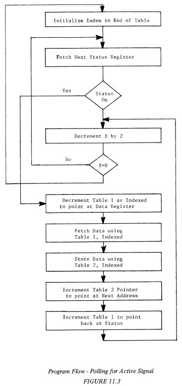
Example 11.8: Polling for Active Signal