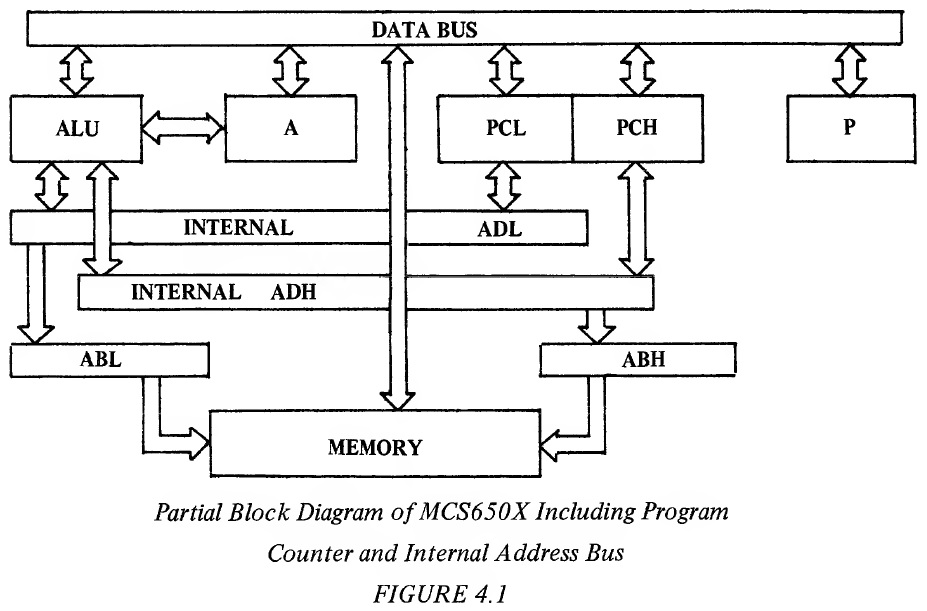
Although two 8 bit registers have been added, they are the only registers in the machine that act as though they are one 16 bit register. They implement a concept known as program count or program sequence and subsequently their value will be referred to as PC or program count. In certain operations it may be convenient to talk about how one affects the program count low (PCL) which will be the lower 8 bit register or the program count high (PCH) which will be the higher 8 bit register. The reason for this register being 16 bits in length is that if it had only 8 bits it would only be able to reference 256 locations. Since it is through the address bus that one accesses memory, the program counter which defines the addressable location, should be as wide a word as possible. The accessing of a memory location is called "addressing". It is Lue selection of a particular eight-bit data word (byte) out of the 65,536 possibilities for memory data locations. This selection is transmitted to the memory through the 16 address lines (ADH, ADL) of the microprocessor. For a more detailed discussion of how an individual memory byte is selected by the address lines, the reader is referred to Chapter 1 of the Hardware Manual. If the program counter was only 1 byte and if the bit pattern which allows the microprocessor to choose which instruction it wants to act on next, such as "LDA" as opposed to an "AND", was contained in one byte of data we could only have 256 program steps. Although the machine of this length might make an interesting toy, it would have no real practical value. Therefore, almost all of the competitive 8 bit microprocessors have chosen to go to a double length program counter. Even though some of the microprocessors of the MCS650X family do not have all of the output address lines necessary to allow the user to address 65K bytes of program (due to package pinout constraints) , in all cases the program counter is capable of addressing a full 65K by virtue of it's 16 bit length. 4.0.1 Use of the Program Counter to Fetch an Instruction The microprocessor contains an internal timing and state control counter. This counter, along with a decode matrix, governs the operation of the microprocessor on each clock cycle. When the state of the microprocessor indicates that a new instruction is needed, the program counter (program address pointer) is used to choose (address) the next memory location and the value which the memory sends back is decoded in order to determine what operation the MCS650X is going to perform next. To use the program counter to perform this operation correctly, it must always be addressing the operation the user wants to perform next. This operation may be an instruction or may be data on which the instruction will operate. In the MCS650X family, the program counter is set with the value of the address of an instruction. The microprocessor then puts the value of the program counter onto the address bus, transferring the 8 bits of data at that memory address into the instruction decode. The program counter then automatically increments by one and the microprocessor fetches further data for address operation necessary to complete the instruction. In the simple example below. Example 4.1: Accessing Instructions with the P Counter Value P Counter* Location Contents 0100** LDA *Program Counter 0101 ADC **Hexadecimal 0102 STA Notation one can see how the program counter is used to access the instruction sequence load A, add with carry, and store the result. In this example, the program counter would start out containing 0100. The microprocessor would read location 0100 by using the program counter to access memory and would then interpret and implement the LDA instruction as previously described. The program counter will automatically increment by one on each instruction fetch, stepping to 0101. After performing the LDA, the microprocessor would fetch the next instruction addressing memory with the program counter. This would pick up the ADC instruction, the add would then be performed, the program counter which has been incremented to 0102 would be used to address the next instruction, STA. The P counter incrementing once with each instruction is an oversimplified view of what actually transpires within the microprocessor. The MCS650X processors usually require more than one byte to correctly interpret an instruction. The first byte of an instruction is called the OP CODE and is coded to contain the basic operation such as LDA (load accumulator with memory) and also the data necessary to allow the microprocessor to interpret the address of the data on which the operation will occur. In most cases, this address will appear in memory right after the OP CODE byte. This allows the microprocessor to use the program counter to access the address as well as the OP CODE. The following example shows how the program counter picks up the instruction and the address of data located at address 5155. Example 4.2: Accessing Data Address With P Counter Value P Counter Location Contents 0100 LDA 0101 55 0102 51 0103 Next Instruction The OP CODE appears in Location Address 0100. The code for the 55 would appear next in Location Address 0101 and the 51 would appear in Location Address 0102, and the OP CODE for the next instruction appears in Location Address 0103. In this example, we see that the program counter is used not only to pick up the operation code, LDA, but is also used to pick up the address of the memory location from which the LDA is going to obtain its data. In this case, the program counter automatically is incremented three times to pick up the full instruction with the microprocessor interpreting each of the individual fetches as the appropriate data. In other words, the first fetch is used to pick up the OP CODE, LDA, the second fetch is used to pick up the low order address byte of the data and the third fetch is used to pick up the high order address byte of the data. This is the form in which many of the microprocessor instructions will appear as it is the most simple form of addressing in the machine and allows referencing to any memory location. Assuming that the microprocessor has the ability to start the program counter at a known instruction, it should be fairly obvious that the program counter would then continue to advance from that location up to the maximum memory location, roll over to the least memory location and continue incrementing through the memory, fetching instructions and addresses as it went. This would give us an interesting sequential program but one which lacked one tremendously powerful concept. The program would have no ability to perform tests or implement various options based on the results of those tests. In the previous section, the concept of flags which are set as a result of the microprocessor operations was developed. To use these flags, the program should be able to test them and then change the sequence of operations which are being performed depending on the result of the test. The program counter is going to continually put out an address, the microprocessor is going to fetch the instruction stored at that address and perform operations based on that instruction. In order to change a sequence of performed instructions by the microprocessor, the programmer must change the value in the program counter. Therefore, test instructions are incorporated which may result in a change of program count sequence as a result of performing one of the tests. The simplest way to change program sequence is to substitute a new value into the program counter location. In the MCS650X microprocessors the simplest way to change the program count sequence is with a JMP instruction. 4.0.2 JMP--Jump to New Location In this instruction, the data from the memory location located in the program sequence after the OP CODE is loaded into the low order byte of the program counter (PCL) and the data from the next memory location after that is loaded into the high order byte of the program counter (PCH). The symbolic notation for jump is (PC + 1)->^PCL, (PC + 2)->PCH. As stated earlier, the "( )" means "contents of" a memory location. PC indicates the contents of the program counter at the time the OP CODE is fetched. Therefore (PC + 2)^PCH reads, "the contents of the program counter two locations beyond the OP CODE fetch location are transferred to the new PC high order byte." The addressing modes are Absolute and Absolute Indirect. The JMP instruction affects no flags and only PCL and PCH. The JMP instruction allows use of the program counter to access the new program counter value as illustrated by the following example: Example 4.3: Use of JMP Instruction (Absolute Addressing Mode) Address Data Comments 0100 JMP Jump to Location 3625 0101 25 (New PCL byte) 0102 36 (New PCH byte) 3625 OP CODE Next Instruction The program counter in the example starts out at location 100. The microprocessor loads a jump instruction. The program counter automatically increments to 101 where the microprocessor picks up and temporarily stores the 25. The program counter automatically increments to 102 where the microprocessor picks up the 36. The 3625 is substituted into the program counter and is used to address the next instruction. Therefore, the JMP instruction contains within its address the new program counter location. Although the jump allows the change of program sequence, it does so without performing my test. So it is a JMP instruction that employed when it is desired to change the program counter no matter what conditions have occurred. Another JMP addressing Mode in the Indirect Addressing Mode. Before this technique can be understood, the basis of indirect addressing found in Chapter 6 must be reviewed. The JMP Indirect instruction is detailed in Chapter 9, page 141. 4.1 BRANCHING To allow for conditional program sequence change, there are a series of branch instructions which test and perform optional changes of the program counter based on the status of the flags. To perform a conditional change of sequence, the microprocessor must interpret the instruction, test the value of a flag, and then change the P counter if the value agrees with the instruction. If the condition is not met, the program counter continues to increment in its normal fashion. Figure 4.2 illustrates how a conditional test might be used.
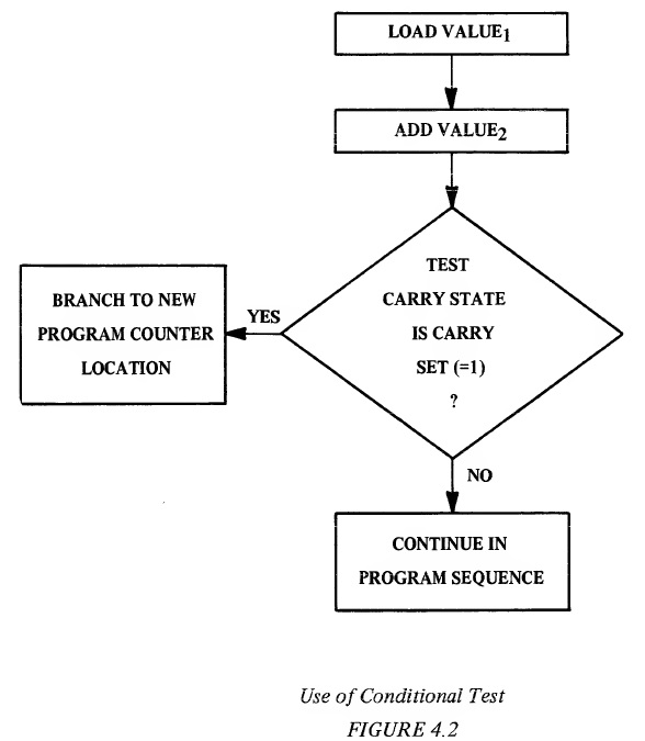
In this example, it is seen that generation of a carry from the add operation will allow an out-of-sequence branch to a new location. 4.1.1 Basic Concept of Relative Addressing If one considers that the instruction JMP required three bytes, one for OP CODE, one for new program counter low (PCL) and one for new program counter high (PCH) it is seen that jump on carry set would also require three bytes. Because most programs for control require many continual jumps or branches, the MCS650X uses "relative" addressing for all conditional test instructions. To perform any branch, the program counter must be changed. In relative addressing, however, we add the value in the memory location following the OP CODE to the program counter. This allows us to specify a new program counter location with only two bytes, one for the OP CODE and one for the value to be added. To illustrate this, in the following example, the branch on carry set (BCS) illustration is followed by a value of 50. If the carry is set, the new program location would be 108 + 50 = 158; in other words, it will take the branch. Example 4.4: Illustration of "Branch on Carry Set" Address Data Comments 0100 LDA Load First Value 0101 ADL1 First Number, low byte 0102 ADH1 First Number, high byte 0103 ADC Add Second Value 0104 ADL2 Second Number, low byte 0105 ADH2 Second Number, high byte 0106 BCS Test for Carry Set. If yes, branch to 0158 0107 +50 0108 STA If not, store results of add 0109 ADL3 Third Number, low byte 010A ADH3 Third Number, high byte 0158 OP CODE New instruction The 0108 represents the value of the program counter after reading the offset value. The program counter automatically increments so it can reference the next memory location on the next cycle. The add of the offset is a signed binary add as discussed in the arithmetic section. A positive branch is indicated by a in bit 7 of the relative value, and a minus branch is in two's complement form and is indicated by a 1 in bit 7. The inherent capabilities of this type of notation system allow branch conditionally forward 127 bytes from the next instruction and back 128 bytes from that instruction. All branches in the MCS650X series are conditional relative branches and all have the form shown above. The advantage of relative addressing is best shown in the following example: Example 4.5: Sequencing Two Branch Instructions Address Data Comments 0100 LDA Load First Value 0101 ADL1 0102 ADH1 0103 ADC Add Second Value 0104 ADL2 0105 ADH2 0106 BCS Test for Carry Set. If yes, branch to 0158 0107 +50 0108 BMI Test for Minus Number. If yes, branch to 0095 0109 -75 010A STA If not, Store 010B ADL3 010C ADH3 In this example, the previous single-branch example was modified to also test the resulting number to see if it is negative. In sequencing two-branch instructions, this loop is 2 bytes shorter by use of relative branches rather than 3 byte branches. 4.1.2 Branch Instructions 4.1.2.1 BMI - Branch on Result Minus This instruction takes the conditional branch if the N bit is set. BMI does not affect any of the flags or any other part of the machine other than the program counter and then only if the N bit is on. The mode of addressing for BMI is Relative. 4.1.2.2 BPL - Branch on Result Plus This instruction is the complementary branch to branch on result minus. It is a conditional branch which takes the branch when the N bit is reset (0) . BPL is used to test if the previous result bit 7 was off (0) and branch on result minus is used to determine if the previous result was minus or bit 7 was on (1). The instruction affects no flags or other registers other than the P counter and only affects the P counter when the N bit is reset. The addressing mode is Relative. 4.1.2.3 BCC - Branch on Carry Clear This instruction tests the state of the carry bit and takes a conditional branch if the carry bit is reset. It affects no flags or registers other than the program counter and then only if the C flag is not on. The addressing mode is Relative. 4.1.2.4 BCS - Branch on Carry Set This instruction takes the conditional branch if the carry flag is on. BCS does not affect any of the flags or registers except for the program counter and only then if the carry flag is on. The addressing mode is Relative. 4.1.2.5 BEQ - Branch on Result Zero This instruction could also be called "Branch on Equal." It takes a conditional branch whenever the Z flag is on or the previous result is equal to 0. BEQ does not affect any of the flags or registers other than the program counter and only then when the Z flag is set. The addressing mode is Relative. 4.1.2.6 BNE - Branch on Result Not Zero This instruction could also be called "Branch on Not Equal." It tests the Z flag and takes the conditional branch if the Z flag is not on, indicating that the previous result was not zero. BNE does not affect any of the flags or registers other than the program counter and only then if the Z flag is reset. The addressing mode is Relative 4.1.2.7 BVS - Branch on Overflow Set This instruction tests the V flag and takes the conditional branch if V is on. BVS does not affect any flags or registers other than the program counter and only when the overflow flag is set. The addressing mode is Relative. 4.1.2.8 BVC - Branch on Overflow Clear This instruction tests the status of the V flag and takes the conditional branch if the flag is not set. BVC does not affect any of the flags and registers other than the program counter and only when the overflow flag is reset. The addressing mode is Relative. 4.1.3 Branch Summary To summarize, the MCS650X branches have two characteristics; each of them tests the state of a flag and then either accesses the next instruction in program sequence if the flag is not in the test state or adds the offset value to the PC value at the OP CODE of the next instruction (PC + 1) to allow the program to change operations. This allows the programmer the full ability to make decisions. By writing a sequence of branch instructions, any combination of conditions of the microprocessor may be determined and new action taken as a result of the tests. There are four branch conditions in the MCS6501-5 microprocessors. These are branch on carry flag, branch of overflow flag, branch on N flag, and branch on zero flag. Each of the branches has a branch on flag set (1) or branch on flag clear (0). 4.1.4 Solution to Branch Out of Range The branch relative instruction is unlike the jump instruction which can reach anywhere in memory, since branch relative is limited to +127 or -128 from the current program counter location. Although for many loops and many tests this is sufficient range, longer programs will occasionally find it necessary to conditionally branch to a location that is significantly further away than the branch command will directly reach. This is one of the uses of complementary branches. If a program should find it necessary to branch to a location which was significantly further away than 127, the following solution would facilitate the branch: Example 4.6: Use of JMP to Branch Out of Range Address Data Comments 100 LDA Load First Value 101 ADL1 102 ADH1 103 ADC Add Second Value 104 ADL2 105 ADH2 106 BCC Branch, if no carry, ahead 3 (to Point 2) 107 +3 108 JMP If carry set, jump to location specified by ADH4, ADL4 109 ADL4 10A ADH4 Point 2 10B BMI Check for Minus 10C Offset 10D STA 10E ADL3 If not minus, Store Result 10F ADH3 In this example, carry set is being checked. In order to accomplish this when the branch command would have to reach outside of the 128 range, the use of a complementary branch is required. Instead of doing the "branch on carry set" to the location, the "branch on carry clear" is utilized (a complementary instruction) which branches past the jump. If the complementary branch is not taken, the jump is the "branch on carry set" function. This technique of branching past a jump with the complementary branch is a universal solution to the branch out of range problem. Another solution is to find a like branch to the same location that is within range and although this involves two branches to transfer control, it does save memory locations. By use of the relative branch less bytes of code are used than if a conditional jump had been used. However, in large programs, the branch out of range occurs more frequently. If the user can determine that a branch will be out of range by inspection, he should use the jump solution at the time he is writing the code. Otherwise, the various assemblers indicate an out of range branch which will require recoding to use the jump solution. NOTE: The jump solution causes 5 bytes of code to be substituted for 2 bytes of branch which in a symbolic assembly may force other branches to go out of range. This might cause several consecutive reassemblies but this technique will solve the problem. 4.2 TEST INSTRUCTIONS Although most of the normal operations of the microprocessor involve setting of flags, there are specific instructions which are designed only to set flags for testing with the branch instruction. 4.2.1 CMP - Compare Memory and Accumulator This instruction subtracts the contents of memory from the contents of the accumulator. Its symbolic notation is A - M. The use of the CMP affects the following flags: Z flag is set on an equal comparison, reset otherwise; the N flag is set or reset by the result bit 7, the carry flag is set when the value in memory is less than or equal to the accumulator, reset when it is greater than the accumulator. The accumulator is not affected. It is a "Group One" instruction and therefore has as its addressing modes: Immediate; Zero Page; Zero Page,X; Absolute; Absolute, X; Absolute, Y; (Indirect, X) ; (Indirect),!. The purpose of the compare instruction is to allow the user to compare a value in memory to the accumulator without changing the value of the accumulator. An example of where this becomes extremely important is when one is receiving command instructions from an external device. In this case, an input byte may have several values. Each value can cause the program to perform a different operation. The only rapid way to determine the value of the input data is to compare the memory with a series of constants. It is fairly simple to perform "compare to constant" operations. By use of the immediate addressing mode which will be developed later, the following example compares an input to three values and branches to different locations for each: Example 4.7: Using the CMP instruction Data Comments LDA Load Value ADL Address Low ADH Address High CMP Compare COUNT 1 to Accumulator COUNT 1 BEQ If Equal, take the branch of OFFSET 1 OFFSET 1 CMP Compare COUNT 2 to Accumulator COUNT 2 BEQ If equal, take the branch to OFFSET 2 OFFSET 2 CMP Compare COUNT 3 to Accumulator COUNT 3 BEQ If equal, take the branch to OFFSET 3 OFFSET 3 Next Inst. Otherwise, go to Next Instruction based on default value (COUNT 4). This example shows how to use the default option. A value was compared against 3 values and if none were equal a fourth, or default value, is assumed. This is a useful technique for code minimization. The compare instruction is designed to allow a signed comparison between 2 values assuming one makes appropriate use of the Z and N and C flags. In order to give maximum flexibility to the instruction, the instruction performs an effective subtract between the value in memory and the value in the accumulator. The reason it is an effective subtract is that subtraction allows the user to compare equal or less with one instruction. The results of a compare are: N C Z V Accumulator < Memory Either Reset Reset Unchanged Accumulator = Memory Reset Set Set Unchanged Accumulator > Memory Either Set Reset Unchanged So, to check if the accumulator is less than memory, the compare is followed by a BCC; to check if equal to is followed by a BEQ; and to check if greater it is followed by a BEQ followed by a BCS. Greater than or equal is checked by BCS. 4.2.2 Bit Testing The comparison instruction is designed for cases when byte or multiple bytes of values are being compared; however, in the analysis of logic functions, it is very often necessary to determine the condition of an individual bit. One of the ways to accomplish this is with the use of the AND instruction as previously discussed. In other words, the user can load a value into the accumulator and AND it with a field that contains a one bit only in the corresponding bit position to the bit under test. By using a Branch on Zero Flag after the AND, the status of the bit in memory is testable by this technique. However, the use of this technique involves destroying the accumulator value with the AND instruction. Therefore, searching a table looking for a single bit in a given position would necessitate the reloading of the test value (mask) after each AND instruction. In order to allow memory sampling without disturbing the accumulator, the BIT instruction is used. 4.2.2.1 BIT - Test Bits in Memory with Accumulator This instruction performs an AND between a memory location and the accumulator but does not store the result of the AND into the accumulator. The symbolic notation is M ^ A. The bit instruction affects the N flag with N being set to the value of bit 7 of the memory being tested, the V flag with V being set equal to bit 6 of the memory being tested and Z being set by the result of the AND operation between the accumulator and the memory if the result is Zero, Z is reset otherwise. It does not affect the accumulator. The addressing modes are Zero Page and Absolute. The BIT instruction actually combines two instructions from the PDP-11 and MC6800, that of TST (Test Memory) and (BIT Test). This, like the compare test, allows the examination of an individual bit without disturbing the value in the accumulator and is illustrated by the example below: Example 4.8: Sample Program Using the BIT Test Data Comments LDA Load MASK into Accumulator MASK BIT Test First Memory Value for Mask Bit ADL1 ADH1 BNE Branch if Set +50 BIT Test Second Memory Value for Mask Bit ADL2 ADH2 BNE Branch if Set -75 etc. The value "MASK" loaded into the accumulator in this example is actually a descriptive title since, this byte is 8 bits, only one of which is a 1. Using this byte in the AND operation inherent in the BIT test will effectively mask out all bits in the memory location under test except that bit position corresponding to the 1 residing in the accumulator. In Example 4.8, the MASK byte is AND'ed to the data found in location ADHl, ADLl and if the bit under test is a 1, the branch will be taken; if not a 1, the second memory location will be tested with the same mask, etc. In addition to the nondestructive feature of the bit which allows us to isolate an individual bit by use of the branch equal or branch no equal test, two modifications to the PDP-11 version of that instruction have been made in the MCS650X microprocessor. These are to allow a test of bit 7 and bit 6 of the field examined with the BIT test. This feature is particularly useful in serving polled interrupts and particularly in dealing with the MCS6520 (Peripheral Interface Device) . This device has an interrupt sense bit in bit 6 and bit 7 of the status words. It is a standard of the M6800 bus that whenever possible, bit 7 reflects the interrupt status of an I/O device. This means that under normal circumstances, an analysis of the N flag after a load or BIT instruction should indicate the status of the bit 7 on the I/O device being sampled. To facilitate this test using the Bit instruction, bit 7 from the memory being tested is set into the N flag irrespective of the value in the accumulator. This is different from the bit instruction in the M6800 which requires that bit 7 also be set on the accumulator to set N. The advantage to the user is that if he decides to test bit 7 in the memory J it is done directly by sampling the N bit with a Bit followed by branch minus or branch plus instruction. This means that I/O sampling can be accomplished at any time during the operation of instructions irrespective of the value preloaded in the accumulator. Another feature of the BIT test is the setting of bit 6 into the V flag. As indicated previously, the V flag is normally reserved for overflow into the sign position during an add and subtract instruction. In other words, the V flag is not disturbed by normal instructions. When the BIT instruction is used, it is assumed that the user is trying to examine the memory that he is testing with the BIT instruction. In order to receive maximum value from a BIT instruction, bit 6 from the memory being tested is set into the V flag. In the case of a normal memory operation, this just means that the user should organize his memory such that both of his flags to be tested are in either bit 6 or bit 7, in which case an appropriate mask does not have to be loaded into the accumulator prior to implementing the BIT instruction. In the case of the MCS6520, the BIT instruction can be used for sampling interrupt, irrespective of the mask. This allows the programmer to totally interrogate both bit 6 and bit 7 of the MCS6520 without disturbing the accumulator. In the case of the concurrent interrupts, i.e., bit 6 and bit 7 both on, the fact that the V flag is automatically set by the BIT instruction allows the user to postpone testing for the "6th bit on" until after he has totally handled the interrupt "for bit 7 on" unless he performs an arithmetic operation subsequent to the BIT operation.