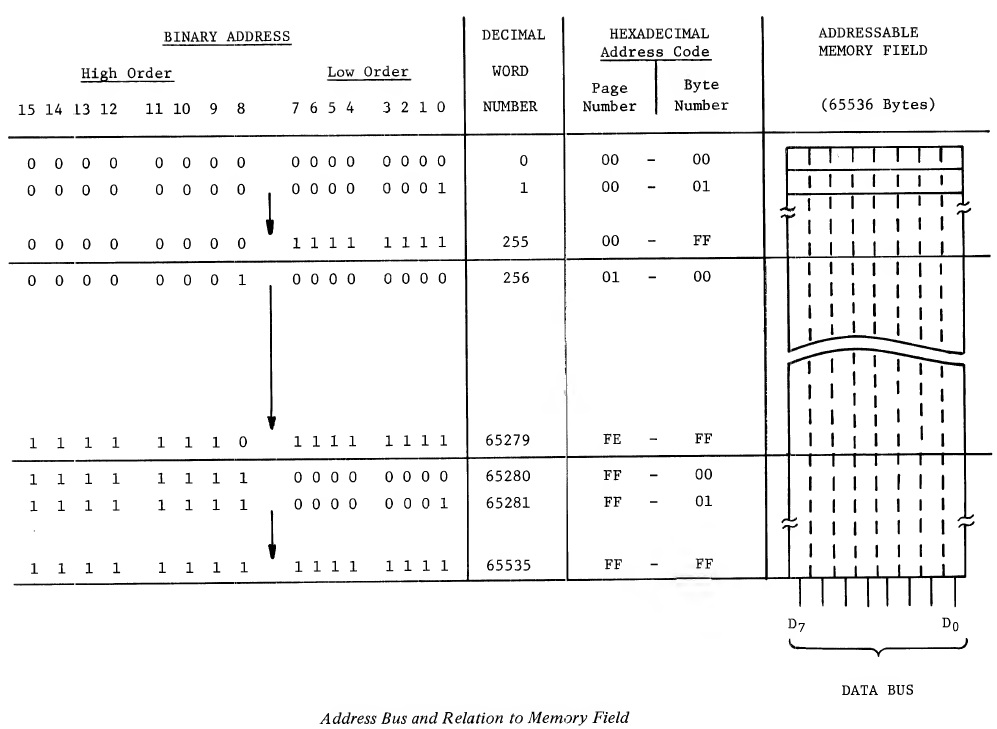
The following example will let us analyze this effect: Example 5.2: Demonstration of "Pipelining" effect Clock Cycles External Operation Address Data Internal Operation 1 Fetch OP CODE 100 ADC Increment P-counter to 101 2 Fetch first-address 101 ADL Increment P-counter half from memory to 102, Interpret ADC instruction 3 Fetch second ad- 102 ADH Increment P-counter dress half from to 103; Hold ADL memory 4 Fetch operand from ADH, Data Load Data memory ADL 5 Fetch next OP CODE 103 STA Increment P-counter memory to 104, Perform ADC operation: A + M + C 6 Fetch address from 104 ADL Increment P-counter memory to 105, Result of Add → accumulator, Interpret STA Instruction The above example shows the operation of an ADC, add with carry instruction, using absolute addressing. In the first cycle, the OP CODE is fetched from memory addressed by the P-counter. To implement the look-ahead or pipeline in cycle two, the fetch of ADL address low is done simultaneously with the interpretation of the ADC absolute instruction. By the end of cycle 2, the microprocessor knows that it should access the next memory location for the address high as a result of interpretation of the absolute addressing mode. The address low (ADL) is stored in the ALU while the address high (ADH) is being fetched in cycle 3. On the fourth cycle, no internal operation is necessary while the microprocessor is putting the calculated value onto the address bus. However, during this cycle, the operand is loaded into the microprocessor. The 4 cycles have all been involved with memory access for the ADC, absolute instruction. The first to fetch the instruction, the second to fetch the address low, the third to fetch the address high and the fourth to use the calculated address to fetch the operand. Because that completes the memory operations for this instruction, during the fifth cycle the microprocessor starts to fetch the next instruction from memory while iL is completing the add operation from the first instruction. During the sixth cycle, the microprocessor is interpreting the new instruction fetched during cycle 5 while transferring the result of the add operation to the accumulator. This means that even though it really takes 6 cycles for the microprocessor to do the ADC instruction, the programmer only need concern himself with the first 4 cycles as the next 2 are overlapped as shown. All instructions take at least 2 cycles; one to fetch the OP CODE and 1 to interpret the OP CODE and, with few exceptions, the number of cycles that an instruction takes is equal to the number of times that memory must be addressed. The details of how each addressing mode is overlapped are described in the individual sections and for specific details of each cycle in various operations, the user is referred to the Hardware Manual, Appendix A. All instructions take at least 2 cycles; one to fetch the OP CODE and 1 to interpret the OP CODE and, with few exceptions, the number of cycles that an instruction takes is equal to the number of times that memory must be addressed. 5.2 MEMORY UTILIZATION As indicated, the 16-bit address allows the user to access greater than 65,000 separate locations. Most of the locations which will be accessed in the course of a control problem will be in program or P-counter referenced locations. A typical program will probably range from 1000 to 8000 bytes and will normally be implemented in fixed ROM or non-volatile alterable ROM. A second type of memory will be the read-write memory in which the user keeps data such as working values, input and output data. Depending on the type of problem being addressed, this RAM usually ranges from 32 bytes to 8000 bytes, although most applications will be under 2000 bytes of RAM. It would seem there is significant address space not used in most applications. To get the maximum benefit of the addressing space, 2 concepts are implemented in the MCS6500 family. These are the use of data addressing as I/O control and distributed address connections for minimum control lines. The latter concept utilizes the address bus, which is basic to and therefore pervasive in any microcomputer system, as a controlling network whenever possible. An example of this is the use of the address bus in selecting devices to interface with the microprocessor. 5.2.1 I/O Control The advantages of accessing I/O as memory are 1) the use of distributed address space allows for simple I/O control lines and 2) all of the power of the instructions is applied to I/O operations. This has the advantage of minimizing I/O hardware and allows the programmer to be innovative in the application of I/O devices in solving his problem. All MCS6500 product family I/O devices contain 8-bit registers which are addressed by the microprocessor as though they were a memory byte. In the simplest case, the 8-bit register being read contains a 1 and 0's pattern which corresponds to the TTL voltage level applied to 8 input pins to the I/O device. If the register was a flip-flop register driving 8 output pins with TTL levels, the storing of 8 bits of data with a STA instruction into that I/O register would, in effect, be programming the flip-flop to a specific desired state. Thus, one can use the instructions with the I/O just as any other memory location. 5.2.2 Memory Allocation Figure 5.1 displays the relationship between memory, address bus and data bus while referencing the address values in hexadecimal notation. The previous section has dealt with utilization of memory address space for not only ROM and RAM but for I/O as well. At this time, the concept of allocation of the memory field of Figure 5.1 to the elements of ROM, RAM and I/O will be considered. The allocation below satisfies most applications requirements and represents an optimum allocation for minimization of programming code and speed. Hexadecimal Address Suggested Allocation of Memory 0000 - 3FFF RAM 4000 - 7FFF I/O 8000 - FFFF ROM It should be noted that the 3 memory blocks address definitions which, while not mandatory or required for proper system operation, do represent a logical assignment of space. The justification for this particular allocation will be presented in Section 9.12. In the meantime, the reader should retain the concept of the various memory blocks allocated to RAM, I/O and ROM as they are useful in the following discussion. With an understanding of pipelining and the concept of memory allocation, the next subject must be: in what manner can data be accessed from the memory field? 5.3 IMPLIED ADDRESSING Implied addressing is a single-byte instruction. The byte contains the OP CODE which stipulates an operation internal to the microprocessor. Instructions utilizing this type of addressing include operations which clear and set bits in the P (Processor Status) register, incrementing and decrementing internal registers and transferring contents of one internal register to another internal register. Operations of this form take 2 clock cycles to execute. The first cycle is the OP CODE fetch and during this fetch, the program counter increments. In the second cycle, the incremented P-counter is now the address of the next byte of the instruction. However, since the OP CODE totally defines the operation, the second memory fetch is worthless and any P-counter increment in the second cycle is suppressed. During the second cycle, the OP CODE is decoded with recognition of its single byte operation. In the third cycle, the microprocessor repeats the same address to fetch the next OP CODE. This is the second time the memory address is fetched; once as the second byte of the first instruction and second, as the correct OP CODE address for the next instruction. A symbolic representation of a 2-cycle instruction is given below. "PC" means "Program Counter." Example 5.3: Illustration of implied addressing Clock Cycle Address Bus Program Counter Data Bus Comments 1 PC PC + 1 OP CODE Fetch OP CODE 2 PC + 1 PC + 1 New Ignore New OP CODE OP CODE; Decode Old OP CODE 3 PC + 1 PC + 2 New Fetch New OP CODE OP CODE; Execute Old OP CODE Instructions which use implied addressing and require only 2 cycles include CLC, CLD, CLI, CLV, DEX, DEY, INX, INY, NOP, SEC, SED, SEI, TAX, TAY, TSX, TXA, TXS, TYA. Instructions utilizing implied addressing and which require more than 2 cycles are stack operations which include BRK, PHA, PHP, PLA, PLP , RTI, RTS. 5.4 IMMEDIATE ADDRESSING Immediate addressing is a 2-byte instruction. The first byte contains the OP CODE specifying the operation and address mode. The second byte contains a constant value known to the programmer. It is often necessary to compare load and/or test against certain known values. Rather than requiring the user to define and load constants into some auxiliary RAM, the microprocessor allows the user to specify values which are known to him by the immediate addressing mode. Example 5.4: Illustration of immediate addressing Clock Cycle Address Bus Program Counter Data Bus Comments 1 PC PC + 1 OP CODE Fetch OP CODE 2 PC + 1 PC + 2 Data Fetch Data, Decode OP CODE 3 PC + 2 PC + 3 New Fetch New OP CODE OP CODE, Execute Old OP CODE Immediate addressing is the simplest form of constant manipulation available to the programmer. It requires a minimum execution time in the sense that 1 cycle is used in loading the OP CODE and as this CODE is being interpreted, the constant is being fetched. Instructions utilizing immediate addressing are ADC, AND, CMP, CPX, CPY, EOR, LDA, LDX, LDY, ORA, and SBC. 5.5 ABSOLUTE ADDRESSING Absolute addressing is a 3-byte instruction. The first byte contains the OP CODE for specifying the operation and address mode. The second byte contains the low order byte of the effective address (that address which contains the data) , while the third byte contains the high order byte of the effective address. Thus the programmer specifies the full 16-bit address and, since any memory location can be modes may be considered special subsets of this 16-bit addressing mode. Example 5.5: Illustration of absolute addressing Clock Cycle Address Bus Program Counter Data Bus Comments 1 PC PC + 1 OP CODE Fetch OP CODE 2 PC + 1 PC + 2 ADL Fetch ADL, Decode OP CODE 2 PC + 2 PC + 3 ADH Fetch ADH, Hold ADL 3 ADH, ADL PC + 3 Data Fetch Data 4 PC + 3 PC + 4 New Fetch New OP CODE OP CODE, Execute Old OP CODE The basic operation of the microprocessor in an Absolute address mode is to read the OP CODE in the first cycle while finishing the previous operation. In the second cycle, the microprocessor automatically reads the first byte after the OP CODE (in this case the address low) while interpreting the operation code. At the end of this cycle, the microprocessor knows that it needs a second byte for program sequence; therefore, 1 more byte will be accessed using the program counter while temporarily storing the address low. This occurs during the third cycle. In the fourth cycle, the operation is one of taking the address low and address high that were read during cycles 2 and 3 to address the operand. For example, in load A, the effective address is used to fetch from memory the data which is going to be loaded in the accumulator. In the case of storing, data is transferred from the accumulator to the addressed memory. As was illustrated in the review of pipelining, depending on the instruction, it is possible for the microprocessor to start the next instruction fetch cycle after the effective address operation and independent of how many more internal cycles it may take to complete the OP CODE. The only exception to this is the case of "Jump Absolute" in which the address low and address high that are fetched in cycle 2 and cycle 3 are used as the 16-bit address for the next OP CODE. The jump absolute therefore only requires 3 cycles. In all other cases, absolute addressing takes 4 cycles, 3 to fetch the full instruction including the effective address, the fourth to perform the memory transfer called for in the instruction. Absolute addressing always takes 3 bytes of program memory; 1 for the OP CODE, 1 for the address low, 1 for the address high, plus 1 byte of data memory (such as RAM) that is pointed to by the effective address. Instructions which have absolute addressing capability include ADC, AND, ASL, BIT, CMP, CPX, CPY, DEC, EOR, INC, JMP, JSR, LDA, LDX, LDY, LSR, ORA, ROL, SEC, STA, STX, STY. 5.6 ZERO PAGE ADDRESSING Zero page addressing is a 2-byte instruction. The first byte contains the OP CODE, while the second byte contains the effective address in page zero of memory. As seen in absolute addressing, the ability to address anywhere in the 65K memory space costs 3 bytes of program space, plus a minimum of 4 cycles to perform address operations. In order to allow the user a shortening of both memory space and execution time, particularly when dealing with working registers and intermediate values, the MCS650X microprocessor family has a special addressing mode that assumes automatically the effective address high (ADH) to be in the lowest page of memory. In order to understand the page concept one should think of each of the various memory addresses as comprising a consecutive block of 256 locations which have an independent high order address associated with that block. Each block is called a page. Other than for zero page and for calculating indexed addresses which will be covered in the following sections, the microprocessor pays little attention to the page concept. The microprocessor assumes that the high order byte of the effective address for instructions which contain OP CODES which indicate the zero page addressing option is all O's (ADH = 00, hexadecimal). This allows the following sequence to occur. Example 5.6: Illustration of zero page addressing Clock Cycle Address Bus Program Counter Data Bus Comments 1 PC PC + 1 OP CODE Fetch OP CODE 2 PC + 1 PC + 2 ADL Fetch ADL, Decode OP CODE 3 00, ADL PC + 2 Data Fetch Data 4 PC + 2 PC + 3 New Fetch New OP CODE OP CODE, Execute Old OP CODE On the first cycle, the microprocessor puts out the program counter, reads the OP CODE and increments the program counter. On the second cycle, the microprocessor puts out the program counter, reads the effective address low, interprets the OP CODE and increments the program counter. So far, the operations are identical to those described in the absolute addressing mode. However, by the end of the second cycle, the microprocessor has decoded the fact that this is a zero page operation and on the next cycle, it outputs address GO, as the effective address high, along with the address low that it just fetched and then either reads or writes memory at that location, depending on the OP CODE. The advantage of zero page addressing is that it takes only 2 bytes, 1 for the OP CODE and 1 for the effective address low; and only 3 cycles, 1 to fetch the OP CODE, 1 to fetch the address low, and 1 to fetch the data, as opposed to absolute addressing which takes 3 bytes and 4 cycles. In order to make most effective utilization of this concept, the user should organize his memory so that he is keeping his most frequently accessed RAM values in the memory locations between and 255. If one organizes the zero page of memory properly, including moving data into these locations for longer loops, significant shortening of program code and execution time can be obtained. The concept of zero page is so important that the various cross assemblers have error notations which indicate when improper use of this space is made. If one's coding is organized according to the guidelines shown in Section 5.2.2, one normally will find working storage located in values from to 255. This is an important aspect of the discipline known as "memory management." Once the pattern of coding for the MCS650X, which considers working storage or registers in the zero page, becomes a habit, one finds that in most control applications, all of the working registers will take advantage of this programming and the associated time reduction without any special effort on the user's part. Instructions which allow zero page addressing include ADC, AND, ASL, BIT, CMP, CPX, CPY, DEC, EOR, INC, LDA, LDX, LDY, LSR, ORA, ROL, SBC, STA, STX, STY. 5.7 RELATIVE ADDRESSING As discussed in Section 4.1, all of the branch operations in the microprocessor use the concept of relative addressing. In example 5.7, it is seen that for the case of the straightforward branch in which the branch is not taken, on the first program count cycle, the microprocessor puts out program counter as an address, fetches the OP CODE and finishes the previous operation. During the second cycle, the program counter is put on the address bus, picking up the relative offset. Internally, the microprocessor is decoding the OP CODE to determine that it is a branch instruction. Example 5.7: Illustration of relative addressing branch not taken External Internal Cycle Address Bus Data Bus Operation Operation 1 0100 OP CODE Fetch Finish Previous Operation, OP CODE Increment Program Counter to 101 2 0101 Offset Fetch Interpret Instruction, Offset Increment Program Counter to 102 3 0102 Next Fetch Next Check Flags, Increment OP CODE OP CODE Program Counter to 0103 This is only the second cycle of an internal operation; therefore, the microprocessor may be storing a computed value from the previous instruction at the same time it is finishing interpreting the present instruction. It is while doing the store operation that the flags in the machine get physically set; therefore, the microprocessor allows the program counter to go 1 more cycle to allow itself time to determine the value of the flags. For examples if the previous instruction is ADC, the flags will not get set until the cycle in which the offset value is fetched. During the third cycle, the microprocessor puts the incremented PC onto the address bus, fetches the next OP CODE and checks the flag in order to decide whether or not the program counter value that is going out is correct and that the branch is not going to be taken. Therefore, an additional type of pipeline, in this case fetching the next OP CODE in a branch sequence, accomplishes the implementation of a branch relative with no branch being taken. This requires 2 cycles. One cycle fetches the branch OP CODE and 1 cycle fetches the next operation, the relative offset. The second fetch is effectively ignored by virtue of the fact that the branch is not taken, so the program counter location has already been incremented and the next OP CODE has already been fetched by the microprocessor. If in the above example it is assumed that the flag is set such that the branch is taken and the relative offset is +50, the microprocessor takes a third cycle to perform the branch operation. Example 5.8: Illustration of relative addressing branch positive taken, no crossing of page boundaries External Internal Cycle Address Bus Data Bus Operation Operation 1 0100 OP CODE Fetch Finish Previous Operation, OP CODE Increment Program Counter to 101 2 0101 +50 Fetch Interpret Instruction, Offset Increment Program Counter to 102 3 0102 Next Fetch Next Check Flags, Add Relative OP CODE OP CODE to PCL, Increment Program Counter to 103 3 0152 Next Fetch Next Transfer Results to OP CODE OP CODE PCL, Increment Program Counter to 153 In Example 5.8, on the first cycle, a branch OP CODE is fetched while the previous operation is finished. On the second cycle, the offset is fetched while the branch instruction is being interpreted. On the third cycle, the microprocessor uses the adder to add the program count low to the offset and also checks the flags. Because the program count for the next OP CODE in program sequence is already in the program counter and is being incremented, the microprocessor can allow the incrementation process to continue. If the value for the next instruction is indicated because the flag is not set , then the microprocessor loads the next OP CODE and the add of the program counter low to the offset value, is ignored as it was in the previous example. If during the third cycle the flag is found to be the correct value for a branch, the OP CODE that has been fetched during this cycle is ignored. The microprocessor then updates the program counter with the results from the add operation, puts that value out on the address bus which fetches a new OP CODE. This gives the effect of a 3-cycle branch. Thus it can be seen that in a case where the branch is not taken, the microprocessor has an effective 2-cycle branch, i.e., 2 memory references. In the case when the branch is taken, the branch takes 3 cycles as long as the relative value does not force an update to the program counter high. In other words, 3 cycles are required if the page boundary is not crossed (recall the discussion of the "page" concept in Section 5.0). If in the above example the branch was back from address 0102 fifty locations, as opposed to +50 locations, the following result would occur: Example 5.9: Illustration of relative addressing--branch negative taken, crossing of page boundaries External Internal Cycle Address Bus Data Bus Operation Operation 1 0100 OP CODE Fetch Finish Previous OP CODE Instruction 2 0101 -50 Fetch Interpret Instruction Offset 3 0102 Next Fetch Next Check Flags OP CODE OP CODE Add Relative to PCL 4 01B2 Discarded Fetch Dis- Store Adder in PCL Data carded Data and Substract 1 from PCH 5 00B2 Next Fetch Next Put Out New PCH OP CODE OP CODE and Increment PC to 00B3 In this example, the adder is used to perform the arithmetic operation, and the adder can do only the 8 bits of addition at a time. The minus branch crosses back over the page boundary, therefore an intermediate result is developed of 01B2 which has no intrinsic value because of the borrow which now has to be reflected into the program counter high. Since this example displays both a negative offset and the crossing of a page boundary, additional explanation is in order. The value to which the offset will be added is 0102 (hexadecimal). The offset itself is -50 (hexadecimal). Subtract low order byte: 02 = 0000 0010 HEX 50 = 0101 0000 HEX Take two's complement of 50: __ 50 = 1010 1111 Add 1 1 -50 = 1011 0000 Add 02 0000 0010 -50 = 1011 0000 Carry = /0/ 1011 0010 B 2 Up to this point, the PCH has not been affected; therefore the value on the address bus is 01B2. The Carry = 0, indicating a borrow. Subtract high order byte: 01 = 0000 0001 HEX 00 = 0000 0000 HEX Take two's complement of 00: _____ 00 = 1111 1111 HEX Add Carry = 0 -00 = 1111 1111 HEX Add 01 0000 0001 -00 1111 1111 Carry = /1/ 0000 0000 0 0 The presence of the Carry indicates no borrow, hence a positive result. At this time, after the arithmetic operation on both bytes of the P.C., the address bus will be: 00B2. The microprocessor does put out on the address line the intermediate results (01B2) , thereby reading a location within the page it was currently working in, the value of which is ignored. It then subtracts 1, or if this was a branch forward to the next page, the microprocessor would add 1 to program counter high in this fourth cycle. In the fifth cycle, the microprocessor will recognize that it has the correct new program counter high and program counter low and is able to start a new instruction operation, thereby giving an effective length to the branch operation when a page crossing is encountered of 4 cycles. It should be noted that all of the above operations are automatic; once a branch instruction is encountered, the following relative value is calculated and put into the memory location after the branch instruction. We can see, however, that it is possible to control the execution time of a branch. This is important for counting or estimating execution times of operations. For counting purposes, the following applies: If a branch is normally not taken, assume 2 cycles for the branch. If the branch is normally taken but it is not across the page boundary, assume 3 cycles for the branch. If the branch is over a page boundary, then assume 4 cycles for the branch. In loops which are repeated many times, one can assume some type of statistical factor between 3 and 2, or 4 and 2, depending on the probability of taking the branch versus not taking it. In order to indicate to the programmer when the 4-cycle branch is taken as opposed to the 3-cycle branch, the various assemblers flag all branch operations which cross page boundaries with a warning message and if timing is important, the user can perhaps relocate his program in such a way that the branch does not cross page boundary. It should be re-emphasized that other than for timing purposes, page boundary crossings can be ignored by the programmer. To summarize, the relative addressing always takes 2 bytes, 1 for the OP CODE and 1 for the offset. The execution time is as follows: Branch with Not Taking the Branch -- 2 cycles Branch When the Branch Is Taken But -- 3 cycles No Page Crossing Branch When the Branch Is Taken with -- 4 cycles a Page Crossing Only branch instructions have relative addressing. The branch instructions are: BCC, BEQ, BIT, BMI, BNE, BPL, BSC, BVC, BVS. For a more detailed explanation of relative offset calculations the reader is referred to Appendix H.